Technical Reference
Port Box
Table of Contents
- Introduction
- Theory of Operation
- Calibration Procedure
List of Illustrations
- Figure 1-1. SuperSALT Assembly
- Figure 1-2. Controller Port Interface Diagram
- Figure 1-3. Current to Voltage Converter Diagram
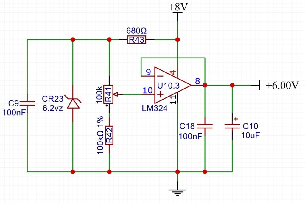
- Figure 1-4. Precision Power Supply Diagram
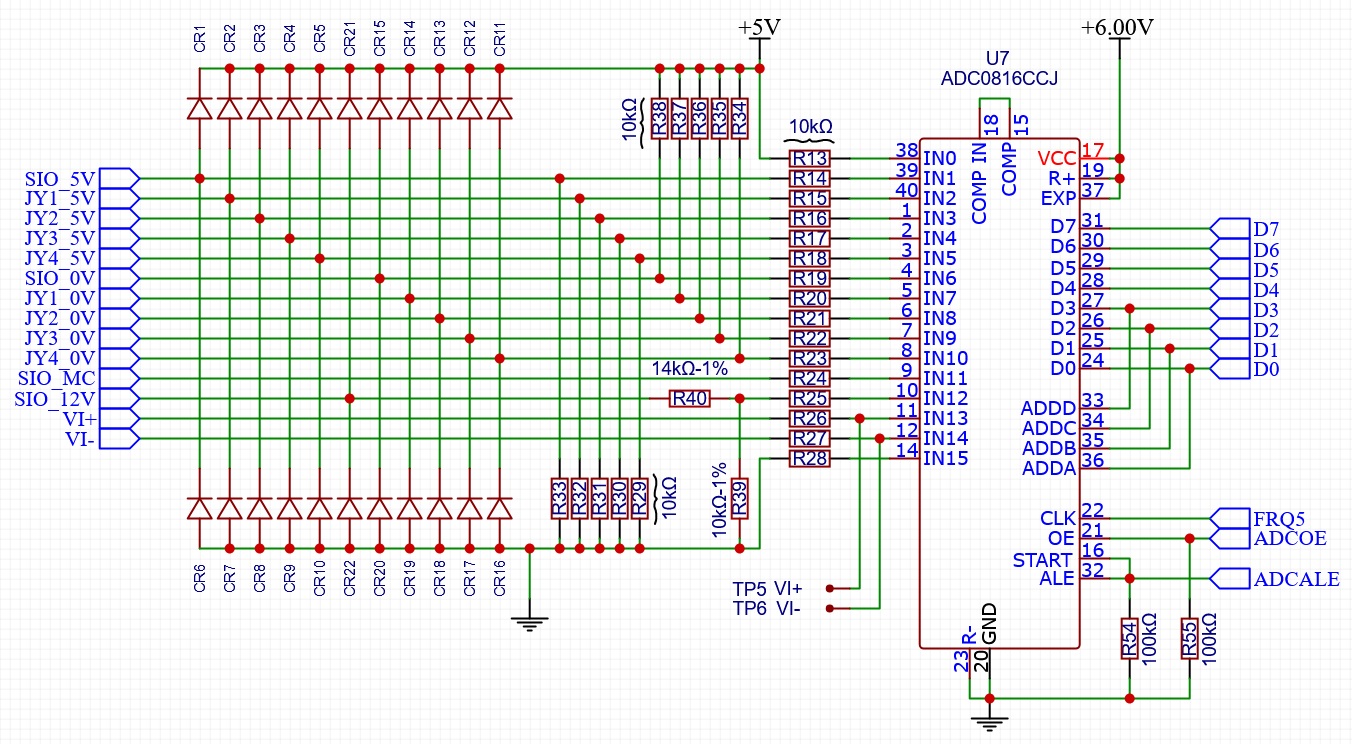
- Figure 1-5. Analog to Digital Converter Diagram
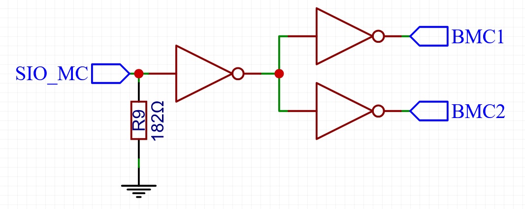
- Figure 1-6. Motor Line Conditioning Circuit
- Figure 1-7. Baud Rate Generator Diagram.
- Figure 1-8. Baud Rate Selector Diagram
- Figure 1-9. Serial Data Generator Diagram
- Figure 1-10. Signal Router Diagram
List of Tables
- Table 1-1. Pot Line to Data Bit Assignments
- Table 1-2. ADC Voltage Test Points
- Table 1-3. Baud Rate Generator Outputs
- Table 1-4. Baud Rate Selection
- Table 1-5. Error Display Port Pinout
Introduction
This reference guide describes the theory of operation and calibration of the CPS SuperSALT Diagnostic Test Assembly (also referred to as the test assembly or port box). It applies to both the original Atari test assembly and the 8Yo Port Box. Based on the original Atari CPS SuperSALT Test Assembly Technical Reference Manual, this edition has been revised to correct technical errors, add clarifying information, and incorporate full-color illustrations and photographs.
Theory of Operation
Overview
The test assembly provides the hardware resources required for the diagnostic software to interconnect ports, generate and route signals, sample voltages, and perform other hardware-assisted diagnostic functions. Together, these capabilities enable the software to thoroughly exercise and verify the external interfaces of the Atari 8-bit console (hereafter referred to as the console).
The diagnostic software controls the test assembly through signals supplied by the unit under test (UUT). Eight programmable data lines (D0-D7) originate from the controller ports, while three control signals (SIO_MC, SIO_OUT, and SIO_CMD) originate from the serial interface. Collectively, these eleven signals form the control interface between the diagnostic software and the test assembly.
Features
The test assembly’s integrated hardware provides the tools needed to thoroughly check and confirm the function of every line in each port of the console. With these built-in capabilities, the system can measure and digitize voltage levels, generate test signals, control signal paths, and send data to the console for analysis.
The Assembly
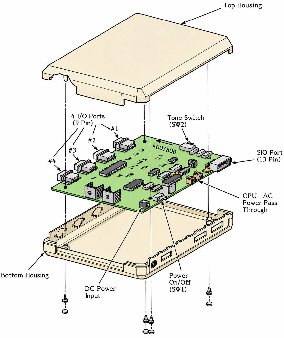
Figure 1-1 illustrates the major components and external connections of the CPS SuperSALT Diagnostic Test Assembly. The remaining sections of this chapter describe the operation of each subsystem in detail.
Figure 1-1. SuperSALT Assembly
The Controller Port Interface
This interface primarily consists of an 8-bit bidirectional data bus formed by the I/O lines of the four controller ports. It serves as the primary communication path between the diagnostic software and the test assembly.
The test assembly requires that all controller ports on the UUT be connected to the corresponding controller ports on the test assembly (see figure 1-1). Every signal line is routed through diagnostic circuitry that allows the software to verify the continuity and operation of each line independently. For this reason, all four controller ports must be connected using 9-conductor cables.
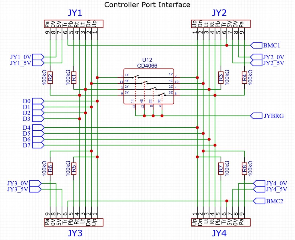
Figure 1-2. Controller Port Interface Diagram
Testing the Data Lines
Figure 1-2 illustrates the test assembly’s controller port interface. The interface is designed to fully exercise the programmable digital I/O capabilities of the console’s 6520 Parallel Interface Adapter (PIA). Each controller port provides access to four bidirectional data lines on pins 1-4. On Atari 400 and 800 systems, the four controller ports collectively expose all sixteen PIA data lines.
As shown in figure 1-2, the corresponding data lines of controller ports 1 and 3, and controller ports 2 and 4, are permanently interconnected. The diagnostic software configures one PIA port as an output and the other as an input, allowing the receiving port to verify that it receives the transmitted data correctly. The test is then repeated with the I/O assignments reversed, confirming proper operation in both directions. To prevent output contention, the software ensures that only one line of each interconnected pair is configured as an output at any time.
On XL/XE systems, where controller ports 3 and 4 are unavailable for general-purpose I/O, the diagnostic software asserts the JYBRG control signal using SIO_MC and SIO_OUT. As shown in figure 1-2, JYBRG enables the quad bilateral switch (U12) to selectively interconnect data lines D0-D3 with D4-D7, providing an equivalent bidirectional data-line test using controller ports 1 and 2.
Testing the Trigger Lines
Each controller port provides one of four trigger lines. As shown in figure 1-2, the trigger lines are driven by the buffered motor control signals BMC1 and BMC2. The diagnostic software verifies each trigger line by toggling SIO_MC and confirming that the corresponding trigger input changes state.
Each controller port provides one of four trigger lines. On the test assembly, the motor control signal (SIO_MC) drives logic buffers whose outputs, BMC1 and BMC2, are connected to the trigger lines (see figure 1-2). The diagnostic software verifies each trigger line by confirming that a change in the state of SIO_MC produces the corresponding change at the trigger inputs.
Testing the Potentiometer Lines
Each controller port provides two potentiometer input lines intended for linear-position controllers (resistive inputs), such as paddles. As shown in figure 1-2, resistors R1 through R8 couple each potentiometer input to a corresponding data line. By driving the associated data line high, the software can individually verify the correct operation of each potentiometer input. The correspondence between potentiometer inputs and data lines is shown in table 1-1.
Table 1-1. Pot Line to Data Bit Assignments
| Pot # | Data Bit | Designation | Resistor |
|---|---|---|---|
| 0 | D3 | P1A | R2 |
| 1 | D2 | P1B | R1 |
| 2 | D7 | P2A | R4 |
| 3 | D6 | P2B | R3 |
| 4 | D1 | P3A | R6 |
| 5 | D0 | P3B | R5 |
| 6 | D5 | P4A | R8 |
| 7 | D4 | P4B | R7 |
Testing the Voltage Supply Lines
Each controller port provides a 5-volt supply line on pin 7 (designated JYn_5V in figure 1-2) and a ground line on pin 8 (JYn_0V). These lines are routed to the analog-to-digital converter (ADC), where their voltage levels can be measured and verified.
The Current to Voltage Converter
The current-to-voltage conversion circuit begins with a 0.1Ω shunt resistor placed in series with the console’s power supply. The sense winding of transformer T1 is connected across this resistor, allowing it to sample the AC current drawn by the console while maintaining electrical isolation from the test assembly. T1 operates in a 1:10 step-up configuration, restoring the signal amplitude reduced by the low-value shunt resistor.
Figure 1-3. Current to Voltage Converter Diagram
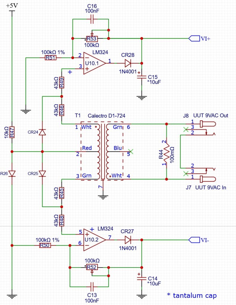
Resistor R47 and diode CR26 are connected in series between +5V and ground, with their junction connected to the center tap of T1’s output winding to establish an artificial ground reference for the AC waveform. This biases the waveform above ground potential, preventing negative excursions that could otherwise produce erroneous readings from U10.
Each half-cycle of T1’s output waveform is rectified by a diode and applied to the non-inverting input of an operational amplifier (op-amp, U10) configured as a peak detector. The filtered DC output is fed back to the inverting input through a 100kΩ resistor, causing the output to track the peak value of the input waveform.
The 100kΩ potentiometer adjusts the feedback voltage, setting the circuit gain. When calibrated with a known load connected to the test assembly, it establishes the current measurement reference.
The outputs of the current-to-voltage converter, designated VI+ and VI- (see figure 1-3), are connected to ADC inputs where they are measured by the software during the Voltage Tests.
Design Note: Transformer T1 used in the original Atari test assembly (Calectro part number D1-724) is a low-power audio output transformer commonly found in 1970s transistor radios, toys, and other battery-powered electronic devices. In its intended application, it matched a transistor amplifier to a small speaker. Atari instead connected the transformer in reverse, using the speaker winding as the input and the amplifier winding as the output. This configuration provides an approximate 10:1 voltage step-up, allowing the small AC voltage across the 0.1Ω current-sense resistor to be amplified before further processing.
The Precision Power Supply
A precision power supply provides 6.00 volts to power the analog-to-digital converter (ADC) and serves as its reference voltage, ensuring accurate measurements.
The circuit (see figure 1-4) consists of op-amp U10 configured as a voltage follower. Its input is derived from the wiper of a 100kΩ precision potentiometer in series with a 100kΩ fixed resistor. This voltage divider is connected across a 6.2-volt zener diode, which provides a stable reference voltage. During calibration, the potentiometer is adjusted to produce an output of 6.00V with a tolerance of ±1%.
Figure 1-4. Precision Power Supply Diagram
The Analog to Digital Converter
The analog-to-digital converter (ADC) is a 16-channel successive-approximation converter. Figure 1-5 shows the ADC circuitry. The ADC is driven by the FRQ5 output of the baud rate generator, which provides the 76.8 kHz EXTCLK signal used to time the conversion cycle when D7 is low.
The ADC measures the voltages present at various points throughout the test assembly and the unit under test (UUT). These voltage test points and their corresponding channel assignments are listed in table 1-2.
Table 1-2. ADC Voltage Test Points
| Ch # | Identifier | Test Point | |||
|---|---|---|---|---|---|
| Schematic | Software | ||||
| 0 | VCC | – | 5 volt line supplying the test assembly | ||
| 1 | SIO_5V | S5+ | 5 volt line from UUT SIO port | ||
| 2 | JY1_5V | P1+ | 5 volt line from UUT controller port 1 | ||
| 3 | JY2_5V | P2+ | 5 volt line from UUT controller port 2 | ||
| 4 | JY3_5V | P3+ | 5 volt line from UUT controller port 3 | ||
| 5 | JY4_5V | P4+ | 5 volt line from UUT controller port 4 | ||
| 6 | SIO_0V | GND | Ground line from UUT SIO port | ||
| 7 | JY1_0V | P1- | Ground line from UUT controller port 1 | ||
| 8 | JY2_0V | P2- | Ground line from UUT controller port 2 | ||
| 9 | JY3_0V | P3- | Ground line from UUT controller port 3 | ||
| 10 | JY4_0V | P4- | Ground line from UUT controller port 4 | ||
| 11 | SIO_MC | MC+ | UUT SIO port Motor control, high-state voltage | ||
| MC- | UUT SIO port Motor control, low-state voltage | ||||
| 12 | SIO_12V | 12+ | 12 volt line from UUT SIO port | ||
| 13 | VI+ | VI+ | Positive half-cycle A/C current draw by UUT | ||
| 14 | VI- | VI- | Negative half-cycle A/C current draw by UUT | ||
| 15 | GND | – | Ground line supplying the test assembly | ||
Figure 1-5. Analog to Digital Converter Diagram
Initiating a Voltage Measurement
Voltage measurements are performed under software control, one channel at a time in rapid succession, while the software interacts with the test assembly through both the SIO interface and the controller port interface. The controller port interface is used to select the ADC channel and configure the baud rate generator to provide the ADC clock. Meanwhile, the SIO command and serial data-out lines control the ADC conversion process.
A measurement is initiated when the software places an encoded byte on the controller port data bus. This value serves two purposes: (1) data bit D7 is driven low to configure the baud rate generator to provide the ADC’s required 76.8 kHz clock (see table 1-4), and (2) data bits D0-D3 specify the channel to be measured. The selected channel is latched into the ADC when the serial data-out line (SIO pin 5) is driven low. Returning the line high starts the conversion while clearing any previous result.
After the conversion is complete, the ADC’s output-enable input is asserted, placing the conversion result onto the data bus where it is read by the software. This is accomplished by driving the SIO command line (SIO pin 7) low, which is normally held high.
Note: This measurement sequence applies to a standard test assembly. Test assemblies fitted with the optional Error Display use a different control sequence, which is described in the Error Display documentation.
The Serial Port Interface
This interface connects to the serial I/O (SIO) port of the UUT. Like the controller interface, it requires a fully wired 13-conductor SIO cable to provide access to every SIO signal required by the diagnostic software. Consequently, a significant portion of the test assembly is dedicated to the circuitry needed to generate, condition, route, and monitor the SIO signals used to exercise the serial interface.
Motor Control Line Conditioning
Figure 1-6 illustrates the conditioning circuitry applied to the Motor Control (SIO_MC) line. A 182Ω pull-down resistor (R9) establishes the input bias while also providing a representative load, allowing the diagnostic software to verify that the console can properly drive the SIO_MC line. The conditioning circuitry converts the resulting signal to TTL-compatible logic levels, producing the internal signals BMC1 and BMC2. These buffered signals can then be distributed to multiple circuits without further loading SIO_MC. The original SIO_MC signal remains available for monitoring by the ADC during diagnostic testing, allowing its voltage to be evaluated under load.
Figure 1-6. Motor Line Conditioning Circuit
Baud Rate Generator
The baud rate generator (U6, MC14411) is a programmable frequency divider. It derives sixteen output frequencies from a single 1.8432 MHz crystal oscillator, all of which are available simultaneously. The test assembly uses six of these outputs to generate the standard communications rates used by Atari 8-bit systems. Data bit D7 selects between the ×1 and ×8 time-base inputs of the MC14411, causing each output frequency to increase by a factor of eight when D7 is asserted. Figure 1-7 shows the baud rate generator circuit, while table 1-3 lists the six outputs and the baud rates they produce for each state of D7.
Figure 1-7. Baud Rate Generator Diagram.
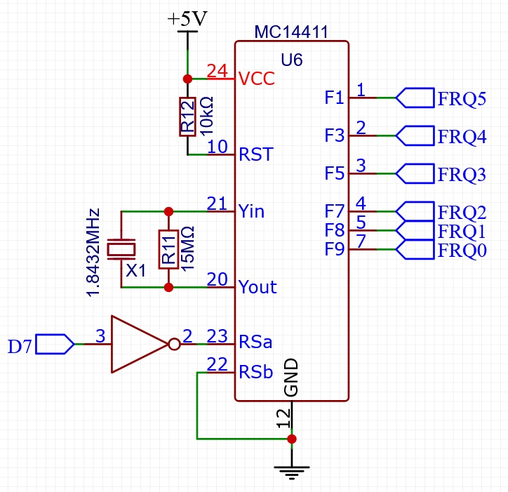
Table 1-3. Baud Rate Generator Outputs
| Output | Baud Rate | ||
|---|---|---|---|
| D7 | D7 | ||
| F1 | FRQ5 | 9600 | 76,800 |
| F3 | FRQ4 | 4800 | 38,400 |
| F5 | FRQ3 | 2400 | 19,200 |
| F7 | FRQ2 | 1200 | 9600 |
| F8 | FRQ1 | 600 | 4800 |
| F9 | FRQ0 | 300 | 2400 |
Baud Rate Selector
The baud rate selector (U5, 74C151) selects one of the six baud rate generator outputs as the active external clock (EXTCLK), according to the state of data bits D4-D6. Figure 1-8 shows the relevant portion of the schematic.
Figure 1-8. Baud Rate Selector Diagram
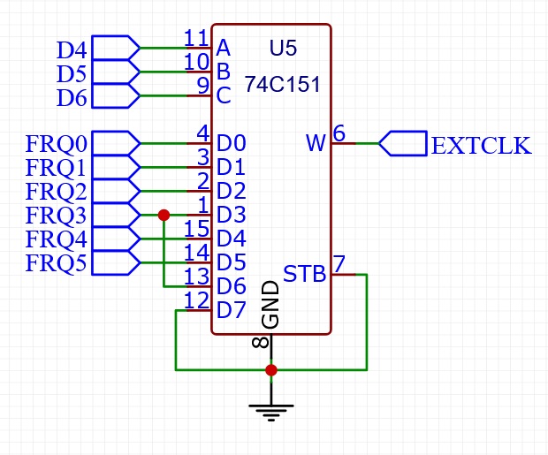
Table 1-4 summarizes the operating modes selected by each combination of D7-D4. The operating modes that differ are shown in bold.
Table 1-4. Baud Rate Selection
| D7 | D6 | D5 | D4 | Baud Rate | |||
|---|---|---|---|---|---|---|---|
| Atari SSA | 8Yo Port Box | ||||||
| 0 | 0 | 0 | 0 | 2400 | 2400 | ||
| 0 | 0 | 0 | 1 | 4800 | 4800 | ||
| 0 | 0 | 1 | 0 | 9600 | 9600 | ||
| 0 | 0 | 1 | 1 | 19,200 | 19,200 | ||
| 0 | 1 | 0 | 0 | 38,400 | 38,400 | ||
| 0 | 1 | 0 | 1 | 76,800 | 76,800 | ||
| 0 | 1 | 1 | 0 | 19,200 | Hi-Z | ||
| 0 | 1 | 1 | 1 | Low | Low | ||
| 1 | 0 | 0 | 0 | 300 | 300 | ||
| 1 | 0 | 0 | 1 | 600 | 600 | ||
| 1 | 0 | 1 | 0 | 1200 | 1200 | ||
| 1 | 0 | 1 | 1 | 2400 | 2400 | ||
| 1 | 1 | 0 | 0 | 4800 | 4800 | ||
| 1 | 1 | 0 | 1 | 9600 | 9600 | ||
| 1 | 1 | 1 | 0 | 19,200 | 19,200 | ||
| 1 | 1 | 1 | 1 | Low | Hi-Z | ||
| *High impedance mode (Hi-Z) electrically isolates the external clock circuit so it does not interfere with the audio signal from the bidirectional clock line during the 2-Way Clock test. | |||||||
Serial Data Generator
The serial data generator produces the external data (EXTDAT) signal from the selected external clock (EXTCLK). As shown in figure 1-9, it consists of a 4-bit binary counter (U4, 74C93) and a 16-input data selector (U3, 74C150). Together, these devices generate a repeating asynchronous serial data stream.
Figure 1-9. Serial Data Generator Diagram
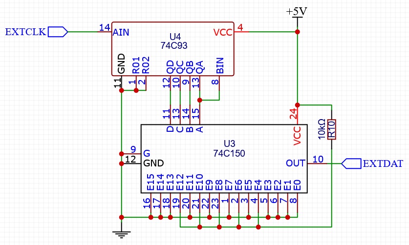
Clocked by the EXTCLK signal, the binary counter repeatedly sequences through sixteen states, addressing successive inputs of the data selector. The selector inputs are hardwired to produce a repeating asynchronous serial frame consisting of one start bit, eight data bits representing hexadecimal value $55, and seven stop bits. The resulting EXTDAT signal is then fed into the signal router.
Signal Router
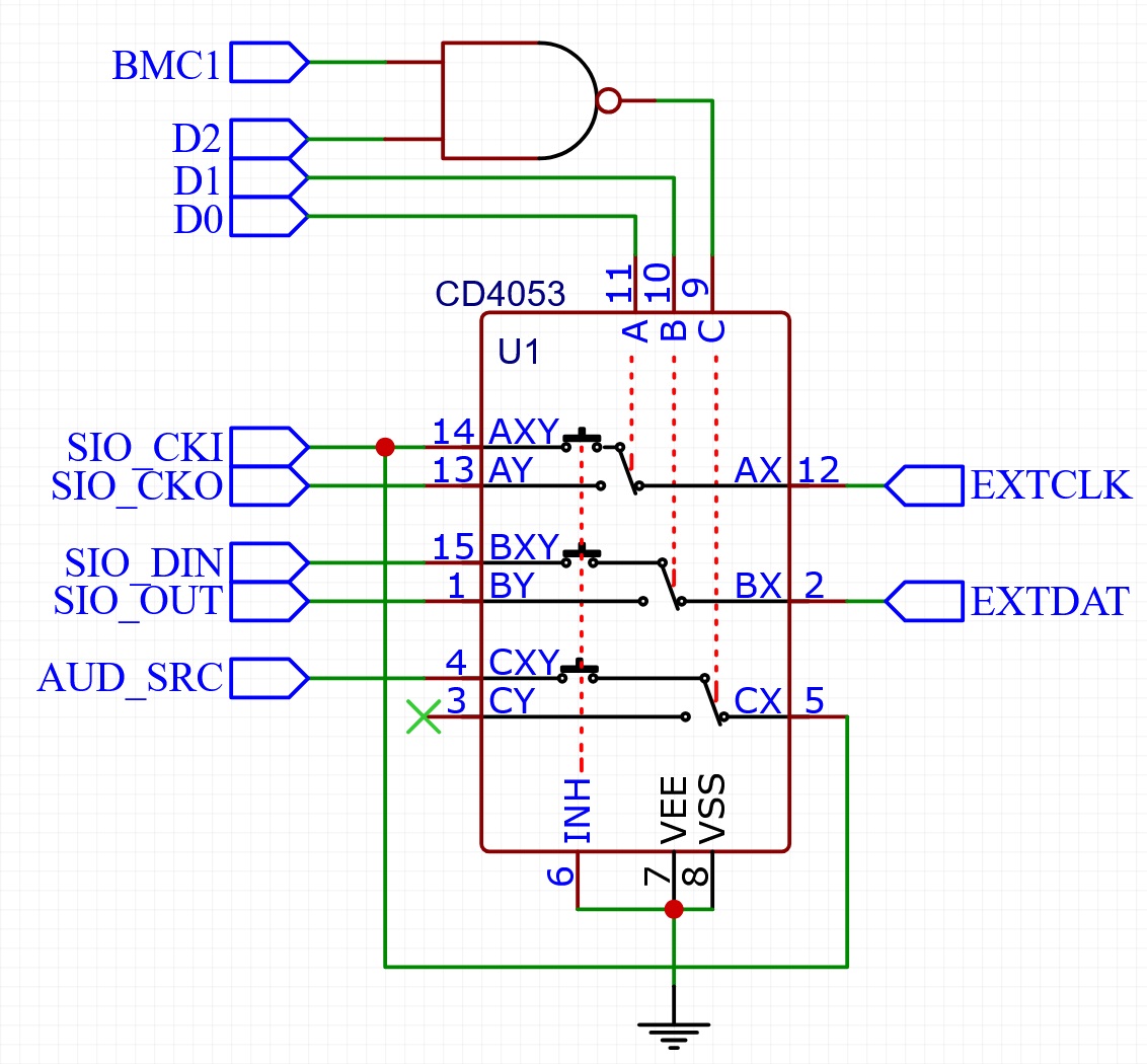
The mode control analog switch (U1, CD4053) contains three independently controllable analog switch sections, each of which is fully bidirectional and electrically isolated from the others (see figure 1-10). Together, these switch sections allow the test software to route signals in a variety of configurations, enabling thorough testing of the serial port lines and their associated functions. The function of each switch section is described below.
Figure 1-10. Signal Router Diagram
U1 Switch Section A
Section A, controlled by data line D0, selects the source signal for the console’s bidirectional serial clock line (SIO_CKI). Depending on the selected operating mode, Section A connects SIO_CKI either to the port-box-generated EXTCLK signal or to the console’s serial clock output (SIO_CKO). The selected signal is also presented to Section C for further routing.
U1 Switch Section B
Section B, controlled by data line D1, selects the source signal for the console’s serial data input line (SIO_DIN). Depending on the selected operating mode, it connects SIO_DIN either to the port-box-generated EXTDAT signal or to the console’s serial data output (SIO_OUT), providing a dynamic data loop-back path.
U1 Switch Section C
Section C selects the source for the audio source (AUD_SRC) signal, which is routed through the tone switch circuit to the console’s serial port audio line. The states of data line D2 and the console’s motor control line (SIO_MC) determine whether AUD_SRC is connected to the console’s bidirectional serial clock line (SIO_CKI) or left disconnected.
The Error Display Port
The error display port (designated J9) provides the signals required by an optional error display board. Table 1-5 shows the pin assignments. Pins that differ are shown in bold.
Table 1-5. Error Display Port Pinout
| Pin | Atari SSA Rev. C | Atari SSA Rev. O | 8Yo Port Box |
|---|---|---|---|
| 1 | D0 | D0 | GND |
| 2 | D1 | D1 | GND |
| 3 | D2 | D2 | D0 |
| 4 | D3 | D3 | D1 |
| 5 | D4 | D4 | D2 |
| 6 | ADCOE | ADCOE | D3 |
| 7 | +8V | +8V | D4 |
| 8 | SIO_OUT | SIO_OUT | D5 |
| 9 | SIO_CMD | SIO_CMD | D6 |
| 10 | BMC1 | BMC1 | D7 |
| 11 | +5V | +8V | ADCOE |
| 12 | GND | GND | BMC1 |
| 13 | D5 | D5 | SIO_OUT |
| 14 | D6 | D6 | SIO_CMD |
| 15 | D7 | D7 | +8V |
| 16 | – | – | +8V |
Calibration Procedure
Proper calibration is essential for accurate voltage measurements and reliable operation of the test assembly. Perform the following procedures before placing the test assembly into service and repeat them periodically to verify continued accuracy.
The following tools and test equipment are required to perform the calibration procedures described in this section.
- Digital Multimeter
- H-90 adjustment tool
- A known-good, stock Atari 800 console equipped with 48 KB of RAM to serve as the load reference.
- 12VDC power adapter
- Pass Thru jumper cable
Important: The original Atari Rev. O test assembly requires a permanent jumper wire be placed on U3 connecting pins 2 and 4. To avoid false baud errors, verify that this jumper is installed before beginning calibration. Install one if necessary.
Set the +6.00V Reference Voltage
Using the H-90 adjustment tool, adjust the +6.00v to +/- 1% precision while measuring between COM and 6.00V taps.
| High Limit | Low Limit |
|---|---|
| +6.06V | +5.94V |
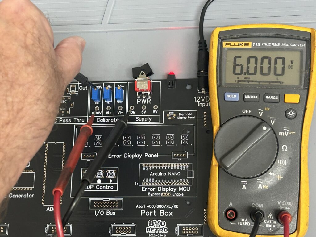
Take your time with this adjustment. The 6.00V reference voltage establishes the calibration of the ADC, so any error here will be reflected in subsequent ADC readings.
Setting the VI+ and VI- baseline requires:
- A known-good, stock Atari 800 console equipped with 48 KB of RAM to serve as the load reference.
- Port Box 12VDC power adapter
- Port Box Pass Thru jumper cable
- H-90 adjustment tool
Establishing the VI+ and VI- Baseline
Connect the Port Box to the Load
- Connect the console’s 9VAC power supply to the AC Pass Thru IN jack on the Port Box.
- Use the jumper cable to connect the AC Pass Thru OUT jack to the 800’s power inlet.
- Switch on the Port Box.
- Ensure there are no cartridges in the 800 console.
- Switch on the 800 and allow it to boot to Memo Pad.
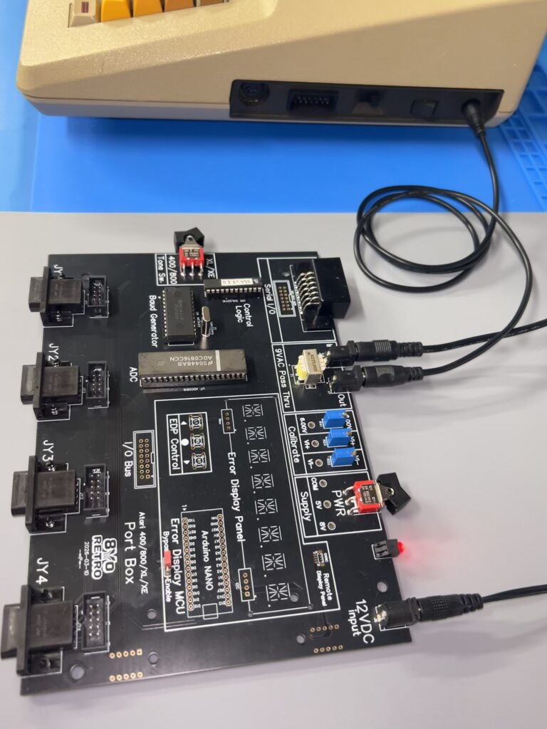
Adjust the VI+/VI− Baseline
Important: The load console must remain idle at the Memo Pad screen throughout this procedure. Do not press any keys or run software, as either will cause excessive VI+/VI− voltage fluctuations that may result in an out-of-spec calibration.
- Connect the COM lead of the DMM to the COM test point and leave it connected throughout this procedure.
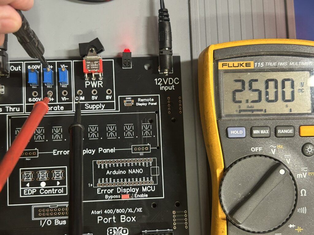
- Connect the DMM positive lead to the VI+ tap and adjust R53 for 2.50V ±1%. A fluctuation of approximately ±15 mV is normal.
- Move the DMM positive lead to VI− and adjust R52 for 2.50V ±1%.
- Repeat steps 2 and 3 until both VI+ and VI− measure 2.50V ±1%.
| High Limit | Low Limit |
|---|---|
| 2.525V | +2.475V |