
Build Guide
Port Box
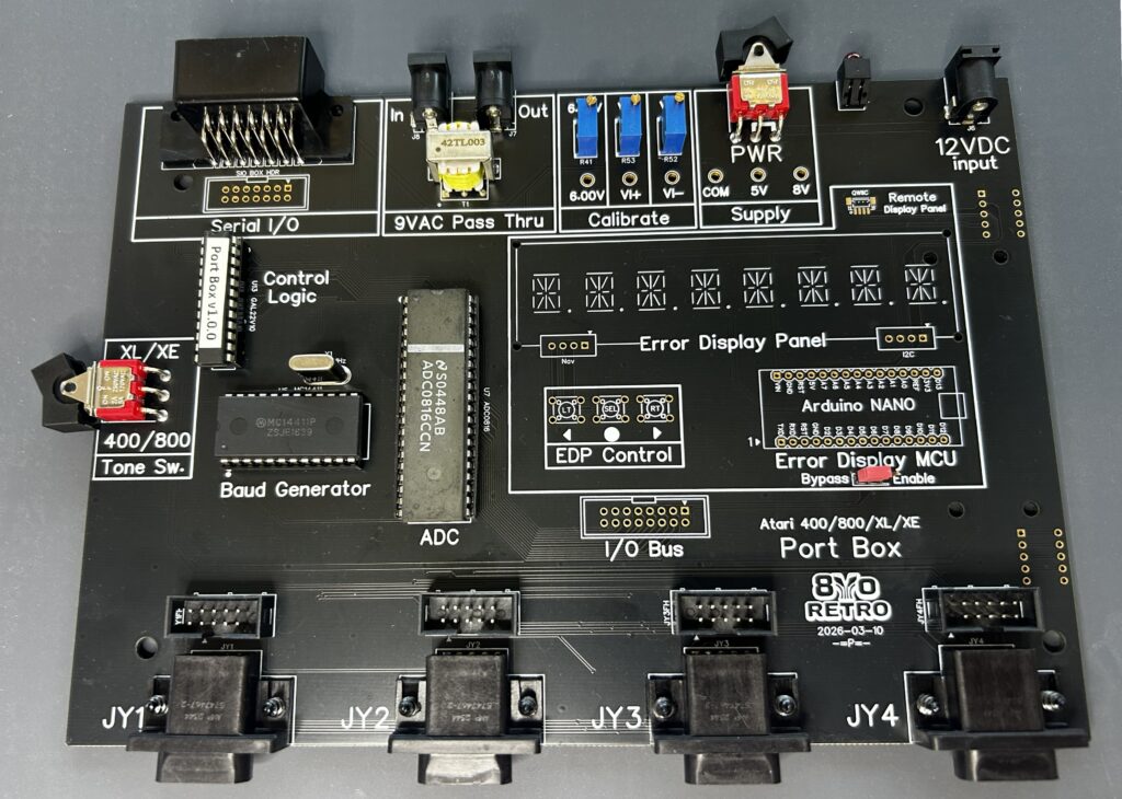
Table of Contents
- About the Port Box
- Before You Begin
- Bill of Materials
- PCB Overview
- Additional Equipment Required
- Port Box Assembly Procedure
- Troubleshooting
About the Port Box
The Port Box is a modern reproduction of Atari’s CPS SuperSALT Test Assembly, originally developed during the early 1980s for factory and field servicing of Atari 8-bit computers. It is supplied as a professionally manufactured printed circuit board (PCB) measuring approximately 150 × 215 mm (5.9 × 8.5 inches).
To simplify assembly, many discrete components have been implemented as factory-installed surface-mount devices (SMDs), reducing the amount of through-hole soldering required. Wherever practical, these SMD components have been positioned away from through-hole solder joints to improve access during assembly and reduce the likelihood of accidentally disturbing nearby components while soldering.
Assembly consists primarily of installing the remaining through-hole components, connectors, switches, and other mechanical hardware, followed by calibration of the completed unit.
These instructions describe the components, assembly procedures, and calibration steps required to complete the Port Box PCB.
Before You Begin
Before committing to this project, it is strongly recommended that you read these instructions in its entirety. Doing so will help you determine whether the assembly is within your skill level and provide a clear understanding of the tools, parts, and procedures involved.
These instructions assume a basic familiarity with through-hole soldering techniques and common electronic assembly practices. The Port Box was designed to be approachable for builders with modest soldering experience; however, fundamental assembly procedures, such as identifying component polarity, forming component leads, trimming excess leads after soldering, and inspecting solder joints for quality, are not described in detail.
Planning Your Build
The builder is responsible for obtaining the following through-hole components, hardware, adapters, cables, enclosure, and external power supply needed to complete the project.
It is recommended to source the required parts in the order of availability, beginning with the legacy components, followed by the equipment required for operation, then finally the standard components.
Bill of Materials
Legacy Components
| Qty | Loc | P/N | Mfr. | Description |
|---|---|---|---|---|
| 1 | J5 | CO12995 | Molex | 13 Pin SIO Connector |
| 1 | U6 | MC14411P | Motorola | Bit Rate Generator (24-pin DIP IC) |
| 1 | U7 | ADC0816CCN | National Semi. | Analog to Digital Converter (40-pin DIP IC) |
| 1 | U13 | GAL22V10D | Lattice | Programmable Logic Device (24 Pin DIP) |
Standard Components
| Qty | Loc. | P/N | Mfr. | Description |
|---|---|---|---|---|
| 1 | T1 | 42TL003-RC | Xicon | Transformer |
| 1 | J6 | 694106301002 | Würth Elektronik | DC Power Jack (5.5 x 2.1mm) |
| 2 | J7,J8 | 694108301002 | Würth Elektronik | DC Power Jack (5.5 x 2.5mm) |
| 4 | JY1-JY4 | 5747467-2 | TE-Connectivity | Right-angle DE-9 Male PCB Connector |
| 4 | JYH1-JYH4 | BHR-10-VUA | Adam Tech | 2×5 (10-pin) Box Header |
| 2 | SW1,SW2 | 300SP1J1BLKM6QE | E-Switch | Rocker Switch, SPDT, ON-ON |
| 1 | J10 | 61300311121 | Würth Elektronik | 3-pin 2.54 mm Header (Bypass shunt header) |
| 1 | JS10 | M7581-05 | Harwin | Jumper Socket (shunt) |
| 1 | LED1 | SSF-LXH100LID | Lumex | PCB LED Indicator |
| 2 | X1 | AB-1.8432MHZ-B2 | Abracon | 1.8432 MHz Crystal |
| 1 | U7 | 4840-6004-CP | 3M | 40-pin DIP Socket |
| 1 | U6 | 4824-6004-CP | 3M | 24-pin DIP Socket |
| 1 | U13 | 4824-3000-CP | 3M | 24-pin DIP Socket (Narrow, 7.62mm) |
| 3 | R41,R52,R53 | 3296W-1-104LF | Bourns | 100KΩ 10-turn Trimmer Potentiometer |
Assembly Tools and Supplies
Below are the tools and supplies you’ll need for assembling the Port Box.
Required Tools and Supplies
- Temperature-controlled soldering iron with a fine tip
- Electronic-grade solder (60/40 or lead-free equivalent)
- Small flush cutters
- Phillips #1 screwdriver
- Digital multimeter (DMM)
- H-90 Adjustment Tool
Recommended Tools and Supplies
- Desoldering braid or solder sucker
- Fine-point tweezers
- Magnifying lamp or head-mounted magnifier
- Isopropyl alcohol and a small brush for cleaning flux residue
- Reusable adhesive putty (Blu Tack® or equivalent)
PCB Overview
The Port Box PCB has two distinct sides. Understanding the purpose of each side before beginning assembly will help ensure that components are installed correctly.
Top Side (Assembly Side)
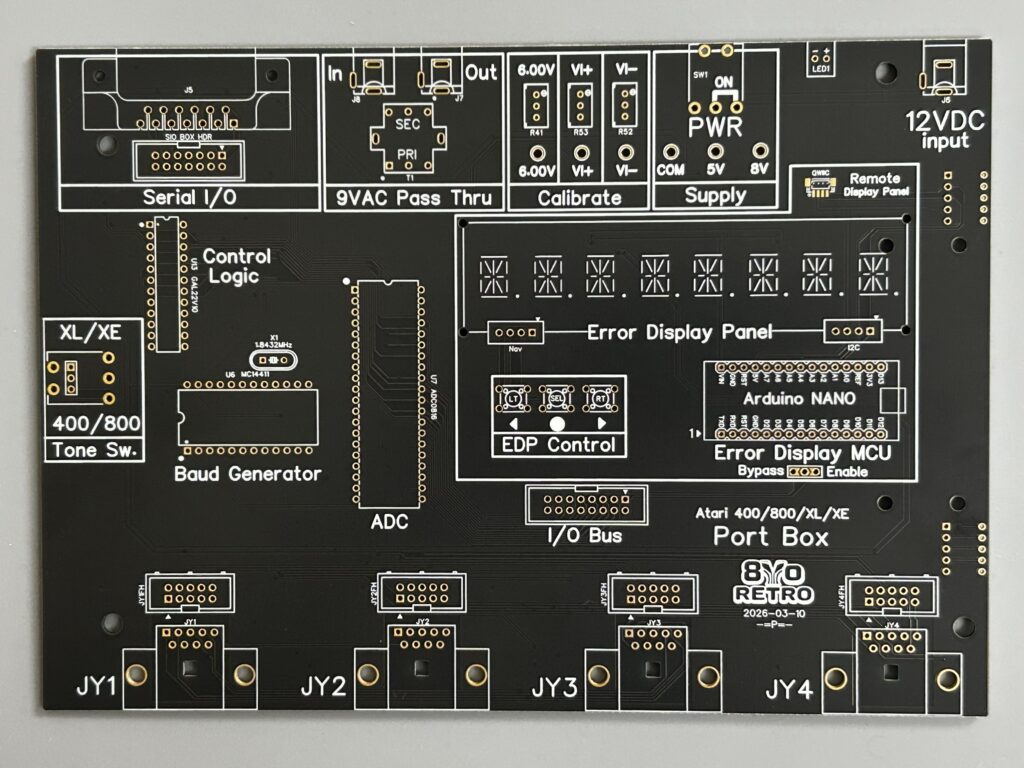
Use this side to identify component locations and orientations before inserting each component into the PCB.
Bottom Side (Solder Side)
The Bottom Side contains the factory-installed surface-mount components. No additional components are installed on this side.
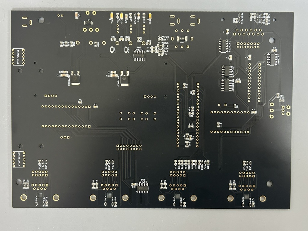
After placing a component into the Top Side of the PCB, carefully turn the board over and solder its leads from the Bottom Side. Take care not to place unnecessary pressure on the factory-installed surface-mount components while handling the board.
Throughout these instructions, the terms Top Side and Bottom Side always refer to the two faces of the PCB, not its position on your workbench.
Unless otherwise noted, photographs and directional references (top, bottom, left, and right) are shown with the Top Side facing upward and the silkscreen text upright and readable.
Additional Equipment Required
The completed test assembly is only one component of the complete diagnostic system. Additional equipment is required before the test assembly can be placed into service. For a complete list of the required equipment, along with setup and operating instructions, see the Port Box User Guide.
Enclosure
Like the original Atari device, this PCB is designed to fit inside an original Atari 850 Interface enclosure. Builders wishing to preserve the original appearance may obtain an Atari 850 interface and repurpose its enclosure by removing the original electronics.
As an alternative to scavenging an original Atari peripheral, you can find designs for a 3D printable enclosure online.
Error Display
The optional Error Display will be documented separately and should not be installed until the Port Box has been fully assembled, calibrated, and functionally verified. The standard assembly procedure assumes the Error Display is not present.
Port Box Assembly Procedure
The voltage regulation circuitry is assembled and verified first, establishing a known-good baseline before the remaining circuitry is installed. This staged approach greatly simplifies troubleshooting should a problem arise.
1. Assemble the Power and Regulation Circuitry
Begin by orienting the PCB on the bench with the top side up.
Install the six through-hole power and regulation components in the upper-right section of the PCB.
- J6 DC power jack
- LED1 Power indicator LED
- SW1 Power switch
- R41,R52,R53 100K-Ohm precision trimmer potentiometer
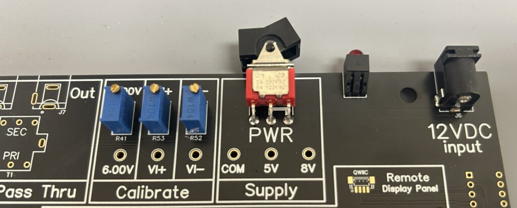
Note: Reusable adhesive putty is particularly helpful for holding through-hole components in position while the PCB is turned over for soldering.
1.1 Test the Power and Regulation Circuitry
The purpose of this early verification is to ensure the power regulation circuitry is operating correctly before additional components are installed. Correcting a fault at this stage is considerably easier than troubleshooting a fully assembled PCB.
Important: Should any of the following checks fail, disconnect power immediately and inspect the assembly before proceeding. Confirm component orientation, solder joints, and part values, paying particular attention to the power jack, power switch, and related circuitry. Do not continue with assembly until the fault has been identified and corrected.
With the power and regulation through-hole components installed, execute the following steps.
- Plug the Port Box 12VDC power adapter into the designated input (J6).
- Set the Port Box power switch to the ON position.
- Verify the power LED is illuminated.
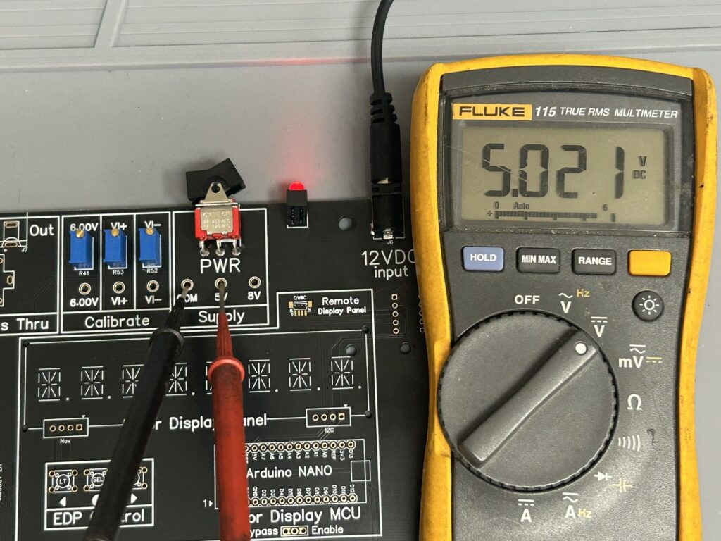
1.1.1 Test the +5V Supply
Verify the fixed +5V rail is within acceptable limits by measuring between the COM and 5V taps.
| High Limit | Low Limit |
|---|---|
| +5.24V | +4.72V |
1.1.2 Test the +8V Supply
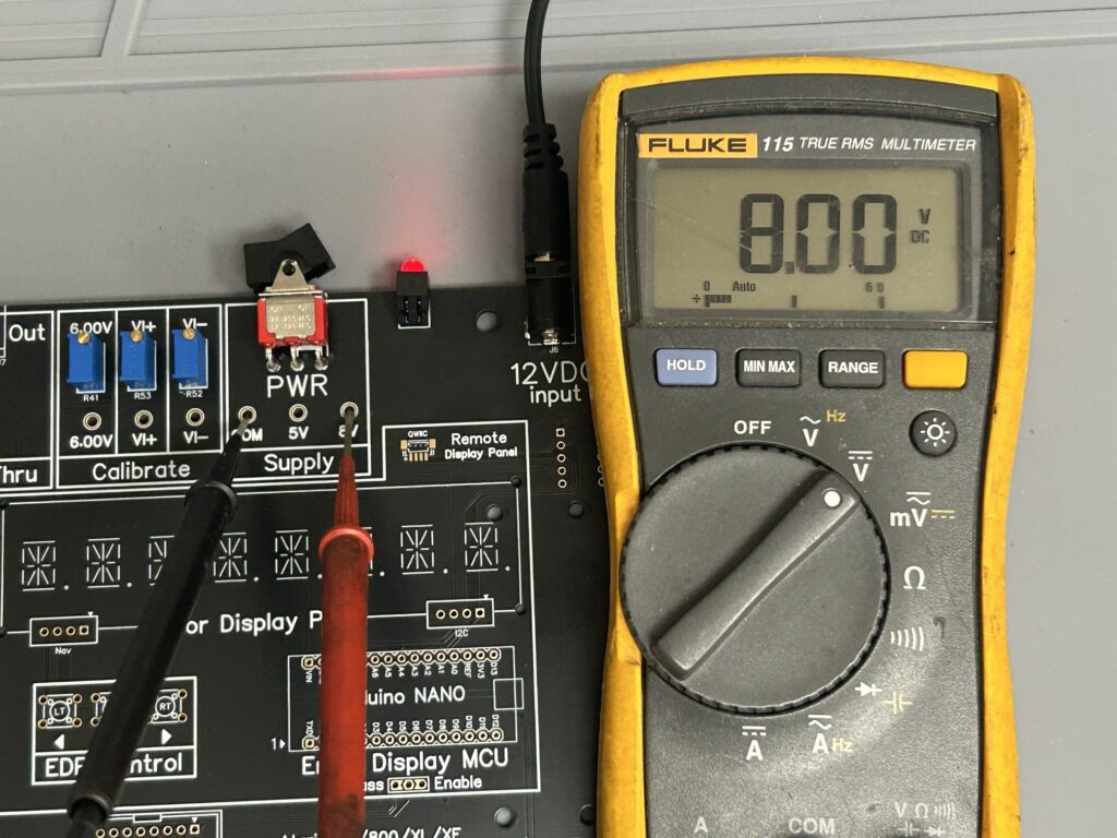
| High Limit | Low Limit |
|---|---|
| +8.40V | +7.60V |
Verify the fixed +8V rail is within acceptable limits by measuring between the COM and 8V taps.
1.1.3 Test the +6.00V Supply
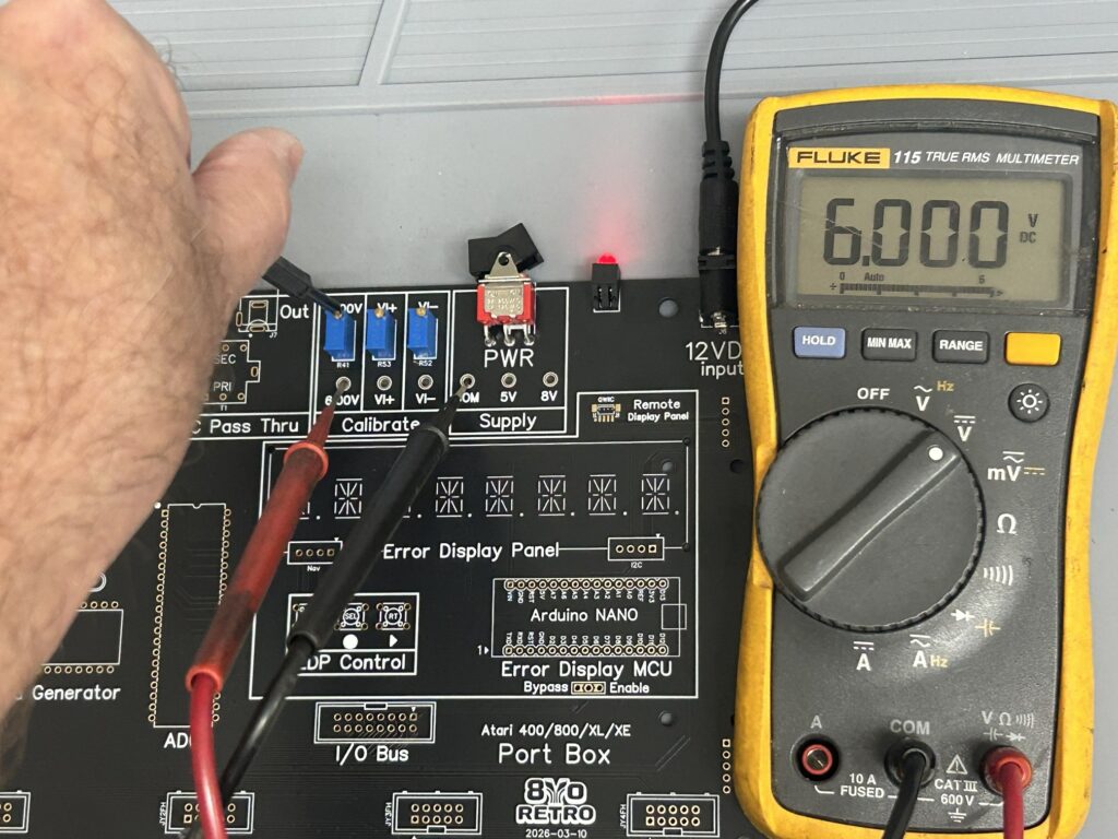
| High Limit | Low Limit |
|---|---|
| +6.06V | +5.94V |
Using the H-90 adjustment tool, ensure that the +6.00v pot adjustment (R41) can be adjusted and remain stable to within specified limits while measuring between COM and 6.00V taps.
2. Assemble the 9VAC Pass Thru Circuitry
This section allows the Port Box to measure a 400 or 800 console’s current draw, when properly connected.
To complete the circuit, install the following 9VAC pass-thru components.
- J7, J8 A/C power jacks
- T1 Transformer
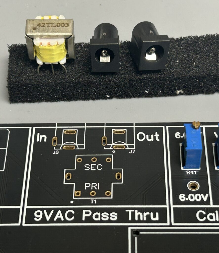
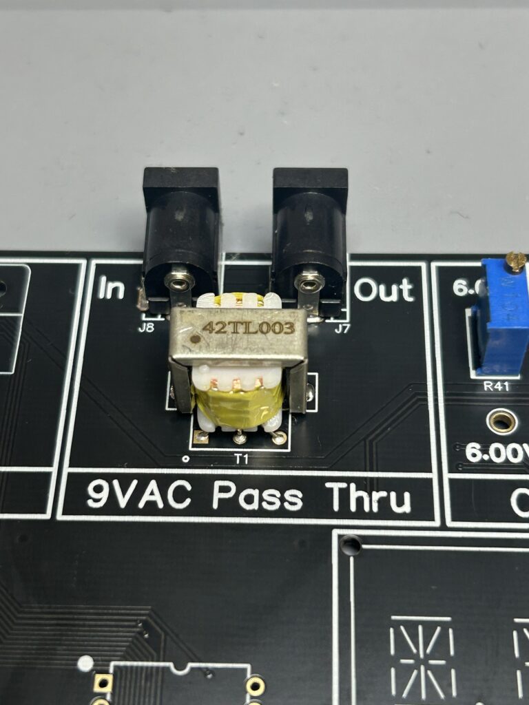
Proper orientation of T1 is essential for correct operation of this circuit, and winding identification markings may vary between manufacturers. On the Xicon 42TL003-RC transformer, the primary winding is identified by a dot. If this marking is absent or unclear, use a digital multimeter (DMM) set to the resistance (Ω) range to measure the resistance across the two outer terminals on each side of the transformer. The primary winding will measure approximately 80Ω, while the secondary winding will measure approximately 1Ω.
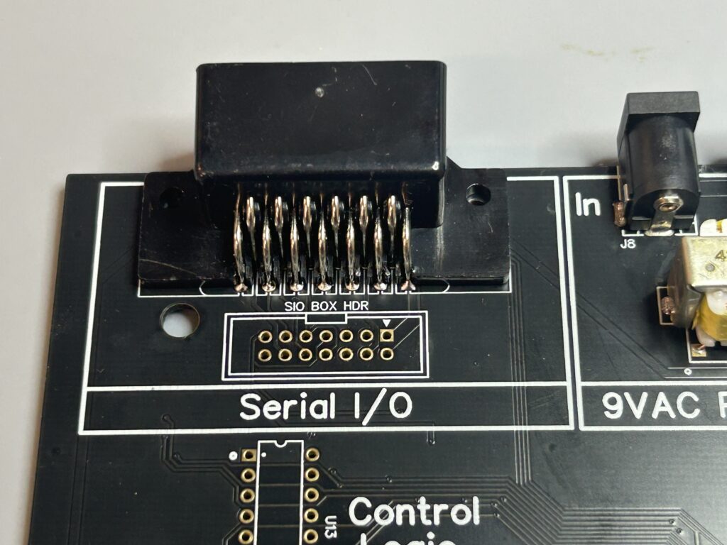
3. Install the SIO Connector
Install the SIO connector at J5 in the upper left corner of the Port Box PCB. It is recommended that the connector be secured with mounting hardware to improve long-term durability.
4. Complete the Controller Port Interface
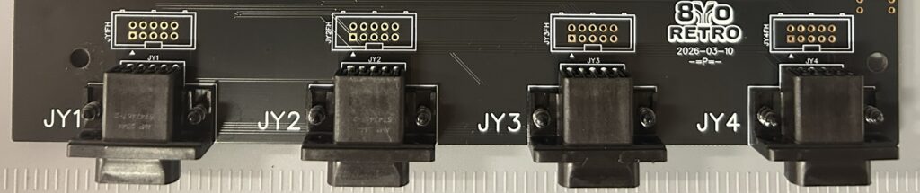
4.1 Install Controller Port Jacks
4.2 Install Controller Port Headers
Installation of the optional JYH1–JYH4 headers is recommended. They provide an inexpensive alternative to the original DE-9 connector arrangement while also serving as a convenient backup should a controller jack or gender changer become damaged.
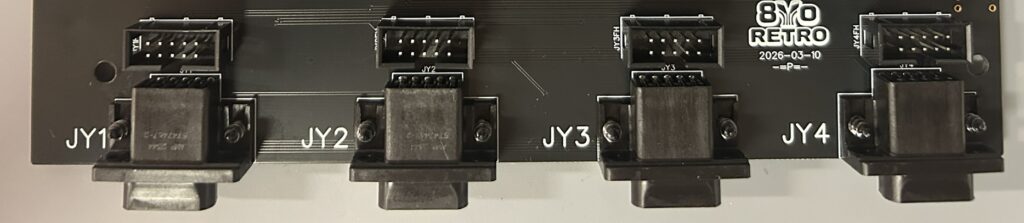
When using the header option, the ribbon cables must either exit through the unused controller-port openings in the enclosure or the enclosure lid must be left off.
5. Install the Error Display Bypass Header and Shunt
Install 3-pin header J10 and shunt JS10.
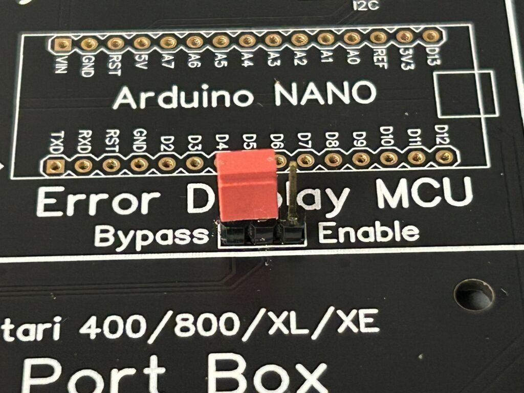
For assembly and initial testing, jumper JS10 must be installed in the Bypass position. The Enable position is intended only for use after the optional Error Display has been installed.
6. Install the remaining components.
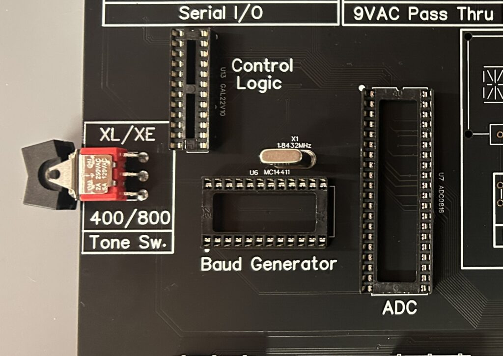
Install the tone switch (SW2), crystal (X1), and IC sockets (U6, U7, and U13).
6.1 Install the Integrated Circuits
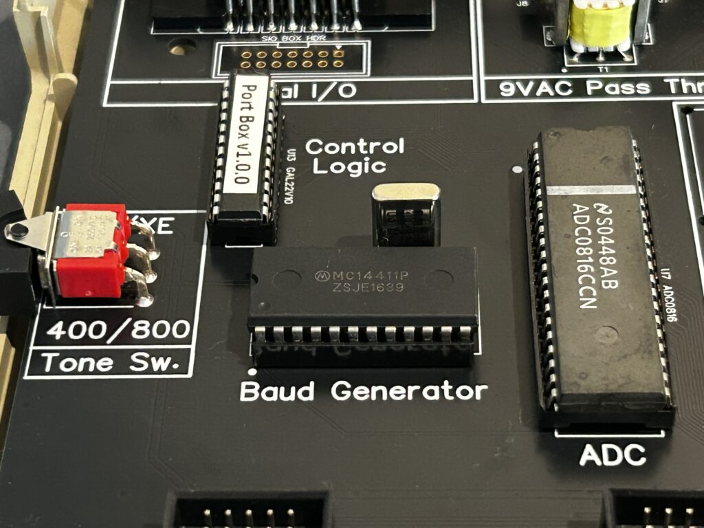
Note: If your port box was not supplied with a preprogrammed GAL22V10, program the device with the appropriate GAL22V10 JEDEC file before installing it at U13 on the PCB.
While observing proper orientation, carefully seat ICs U7, U6 and U13 in their respective sockets.
Calibration
Before the test assembly can be placed into service, it must be calibrated to establish the reference voltages and operating conditions required for accurate diagnostic testing. Because the calibration procedure applies equally to both the original Atari test assembly and the 8Yo Port Box, it is documented in the Technical Reference.
Troubleshooting
If a problem is encountered during assembly or verification of the port box, refer to the following table for recommended corrective actions based on the observed symptom.
| Symptom | Recommended Action |
|---|---|
| +5V and/or +8V are out of specification. | 1. Verify that the external power supply is rated for 12VDC 2A (2000mA) with a center-positive barrel connector. 2. Inspect SW1 and J6 for proper installation and soldering. 3. Check for unsoldered pins, solder bridges, solder splashes, and cold solder joints in the power input circuitry. |
| +5V and +8V are within specification, but the +6.00 V reference cannot be adjusted to specification. | 1. Verify that R41 is installed and is 100K-ohms (often marked, “104”). 2. Inspect the +6.00 V reference circuitry for solder defects, damaged PCB traces, and damage to the factory-installed SMD components on the reverse side of the PCB. |
| A measured voltage is unstable or fluctuates. | 1. Inspect the associated circuitry for poor solder joints, solder bridges, damaged traces, and damaged or incorrectly installed components. 2. Verify that the test leads are making reliable contact with the measurement points. |
| A verification or calibration step cannot be completed. | 1. Perform a thorough visual inspection of both sides of the PCB. Compare your completed assembly with the top and bottom PCB images provided in the PCB Overview section. Pay particular attention to the factory-installed SMD components on the reverse side of the PCB. 2. Verify component orientation, component values, solder joints, and PCB condition before attempting further troubleshooting. |